



Key Findings
- For 30 years after red and green LEDs, blue LEDs remained an elusive holy grail needed to synthesize white light.
- Shuji Nakamura defied industry consensus by choosing GaN over ZnSe and engineering the two-flow MOCVD reactor.
- Thermal annealing under pure nitrogen solved the 30-year p-type GaN doping mystery caused by hydrogen passivation.
- Pairing blue InGaN LEDs with yellow YAG phosphor sparked an energy revolution, cutting global lighting energy by over 40%.
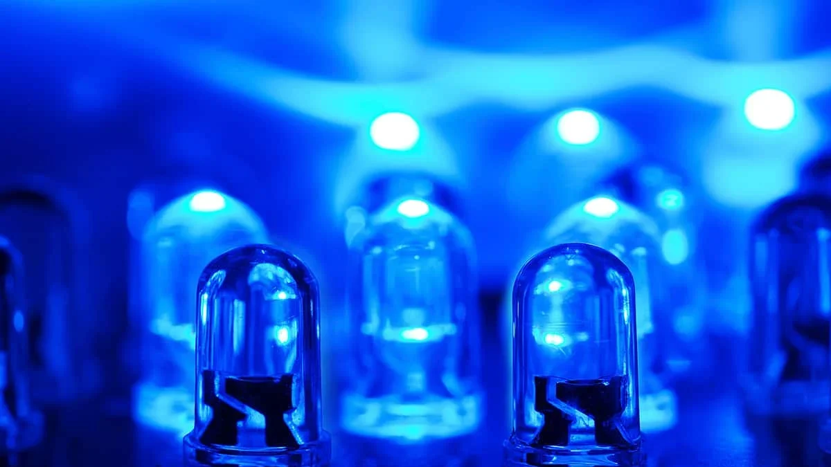
Pick up a modern smartphone, gaze at a razor-thin 4K television screen, or switch on an energy-saving household lightbulb, and you are witnessing one of the most improbable triumphs in the history of solid-state physics: the blue light-emitting diode (LED) [1, 4]. For three long decades following the invention of red and green LEDs in the 1960s, creating an efficient, high-brightness blue semiconductor diode was universally regarded as an impossible scientific frontier. Industrial conglomerates, including IBM, Bell Labs, GE, RCA, Sony, and Matsushita, poured hundreds of millions of dollars and decades of elite research into solving the blue LED puzzle, only to abandon their programs in bitter defeat [3].
Without blue light, however, the digital revolution was fundamentally incomplete. In optical physics, combining red, green, and blue (RGB) wavelengths is the absolute prerequisite for synthesizing white light and rendering the entire color gamut across digital displays. While conventional incandescent bulbs wasted over 90 percent of their electrical energy as heat, creating an efficient solid-state white light source promised to cut global energy consumption by a staggering margin [4]. The breakthrough did not emerge from a sprawling Silicon Valley campus or a corporate tech titan; it was cracked in a tiny, modest Japanese chemical firm by a tenacious engineer named Shuji Nakamura, working alongside academic pioneers Isamu Akasaki and Hiroshi Amano, an achievement recognized with the 2014 Nobel Prize in Physics [1, 2, 3].
The Missing Primary Color: The 30-Year Quest for Blue Light
The journey of light-emitting semiconductors began in 1962 when General Electric engineer Nick Holonyak Jr. developed the first practical visible-spectrum red LED using gallium arsenide phosphide (GaAsP). A few years later, researchers at Monsanto successfully synthesized green LEDs using nitrogen-doped gallium phosphide (GaP). These early LEDs quickly established dominance in electronic indicator lights, digital watches, and pocket calculators. However, for everyday illumination, human civilization remained dependent on Thomas Edison’s hundred-year-old incandescent filament bulbs and toxic mercury-filled fluorescent tubes [3, 4].
To produce clean white light or generate high-resolution full-color video displays, optical engineering requires additive color mixing: simultaneous red, green, and blue photons. Because photon energy is inversely proportional to wavelength (governed by the Planck-Einstein relation, E = hc / lambda), blue light requires significantly higher energy (roughly 2.7 to 3.1 electron volts) than red light (1.8 electron volts) or green light (2.2 electron volts). For thirty years, every attempt to force semiconductor materials to emit high-intensity photons in this high-energy spectral band collapsed into non-radiative heat dissipation and structural crystal degradation [1, 3].
Semiconductor Physics: How p-n Junctions Generate Photons
To understand why blue emission was so difficult to achieve, one must examine the solid-state physics of a p-n semiconductor junction. An LED is a specialized semiconductor diode composed of two distinct electrical zones: an n-type layer doped with extra electrons, and a p-type layer doped with electron deficiencies known as ‘holes’ [1].
When an electrical voltage is applied in forward bias, electrons from the n-side and holes from the p-side are driven toward the microscopic junction boundary. When a free conduction-band electron encounters a valence-band hole, they recombine in a quantum transition. As the electron falls across the semiconductor’s forbidden energy bandgap, it releases its surplus potential energy as a single packet of electromagnetic radiation: a photon. The physical width of this energy bandgap determines the exact color of the emitted light. To generate blue photons with a wavelength between 450 and 470 nanometers, physicists needed a semiconductor crystal possessing a wide, direct bandgap exceeding 3.2 electron volts, a material property notoriously difficult to synthesize [1, 3].
Forward Voltage
Electrical current drives conduction-band electrons from the n-layer and valence holes from the p-layer into the quantum well.
Radiative Decay
Electrons drop into vacant electron holes across the 3.4 eV wide direct bandgap of the InGaN crystal active region.
Blue Light Emission
Energy is emitted directly as high-energy blue electromagnetic waves with a sharp wavelength peak around 450 nanometers.
White Illumination
A portion of blue light excites a yellow YAG:Ce phosphor coating, combining to synthesize radiant, high-CRI white light.
Gallium Nitride vs Zinc Selenide: Shuji Nakamura’s High-Stakes Gamble
By the late 1980s, the global physics community had split into two rival camps regarding candidate materials for blue emission: zinc selenide (ZnSe) and gallium nitride (GaN). Virtually all major university laboratories and corporate titans chose zinc selenide because its lattice constant closely matched available gallium arsenide (GaAs) substrates, making thin-film crystal growth relatively straightforward. However, ZnSe possessed weak chemical bonds; under electrical current, crystal dislocations multiplied rapidly, causing devices to burn out within minutes [3].
Conversely, gallium nitride (GaN) possessed immense bond strength, robust thermal stability, and a wide direct bandgap of 3.4 electron volts. Yet GaN was universally despised as an experimental nightmare. There was no substrate in the world that lattice-matched GaN; growing GaN on sapphire resulted in a massive 16 percent lattice mismatch and billions of structural dislocations per square centimeter. Furthermore, nobody in thirty years had ever succeeded in producing p-type GaN, rendering a functional p-n junction theoretically impossible [1, 2].
Shuji Nakamura was an engineer at Nichia Chemical Industries, a modest company in rural Tokushima, Japan, that produced phosphors for fluorescent lamps. Frustrated by competing with corporate giants in saturated commodity markets, Nakamura made a daring calculation: if he worked on ZnSe, he would be crushed by better-funded corporate competitors; but if he tackled GaN, virtually no one was working on it because everyone believed it was a dead end. In 1988, Nakamura boldly persuaded Nichia’s visionary founder, Nobuo Ogawa, to invest 500 million yen (nearly 15 percent of annual revenue) into customized semiconductor hardware [1, 3].
The Two-Flow MOCVD Breakthrough: Growing Pure GaN Crystals
Commercial Metalorganic Chemical Vapor Deposition (MOCVD) systems blasted reactant gases horizontally across heated sapphire substrates. In conventional chambers, the extreme thermal convection plumes rising from the 1,000-degree-Celsius substrate pushed the reactant gases (trimethylgallium and ammonia) away before they could deposit, resulting in fragmented, uneven GaN films riddled with cracks [1].
Nakamura spent months physically modifying the quartz reactor tubes with a blowtorch, designing his legendary ‘two-flow MOCVD’ system. He introduced a secondary, high-velocity perpendicular gas stream of nitrogen and hydrogen that pushed the horizontal reactant gas stream down directly onto the sapphire surface. This dual-flow geometry suppressed thermal convection, allowing smooth, uniform, defect-free single-crystal GaN layers to nucleate on low-temperature aluminium nitride (AlN) or GaN buffer layers. For the first time in scientific history, pristine specular GaN films were achieved with microscopic electrical uniformity [1, 3].
Zinc Selenide (ZnSe) Paradigm
Substrate Match: Excellent lattice match with standard GaAs substrates.
Chemical Bonding: Weak ionic bonding prone to rapid dislocation propagation.
Operational Lifespan: Burned out in minutes to hours under forward continuous bias.
Industry Consensus: Championed by Sony, IBM, 3M, and Bell Labs throughout the 1980s.
Gallium Nitride (GaN) Breakthrough
Substrate Match: Severe 16% lattice mismatch on sapphire conquered by two-flow MOCVD.
Chemical Bonding: Ultra-strong covalent bonding resisting defect degradation.
Operational Lifespan: Continuous commercial lifespan exceeding 50,000 to 100,000 hours.
Industry Consensus: Championed independently by Akasaki, Amano, and Nakamura to win the Nobel Prize.
Solving the p-Type Doping Puzzle: Thermal Annealing Innovation
Even with high-quality GaN films, the ultimate semiconductor roadblock remained: achieving p-type conductivity. When researchers added magnesium (Mg) atoms to GaN to act as electron acceptors, the material stubbornly remained electrically non-conductive. In 1989, Nagoya University researchers Isamu Akasaki and Hiroshi Amano discovered that irradiating Mg-doped GaN with low-energy electron beam irradiation (LEEBI) under an electron microscope unlocked p-type conductivity [3]. However, LEEBI was slow, penetrated only a few nanometers, and was commercially impractical for mass production [2].
Nakamura investigated the underlying chemistry and unmasked the true culprit: hydrogen passivation. During MOCVD crystal growth, ammonia (NH3) dissociated into nitrogen and hydrogen; the reactive hydrogen atoms bonded with magnesium acceptors, neutralizing their positive charge. Nakamura realized that LEEBI simply knocked hydrogen atoms loose via electron impact. Reasoning thermodynamically, Nakamura heated the Mg-doped GaN wafers in a simple furnace to 700 degrees Celsius under a pure nitrogen atmosphere (free of hydrogen). The thermal annealing drove the hydrogen gas out of the crystal lattice completely, activating 100 percent of the magnesium acceptors across the entire wafer [2]. This simple, elegant thermal process unlocked commercial p-type GaN manufacturing worldwide [1, 2].
From Blue Photons to Pure White Light: The YAG Phosphor Miracle
In 1993, Nakamura integrated indium into the crystal lattice to synthesize thin indium gallium nitride (InGaN) quantum wells, which adjusted the bandgap to emit dazzling, high-brightness blue light that was one hundred times brighter than any prior laboratory device [1]. The final step was converting this intense blue light into comfortable, omnidirectional white illumination for human homes and streets.
Instead of assembling three separate and expensive red, green, and blue diodes, lighting engineers coated a blue InGaN chip with a microscopic slurry of cerium-doped yttrium aluminium garnet (YAG:Ce) phosphor [4]. When the high-energy blue photons strike the phosphor, a portion of the blue light is absorbed and re-emitted via Stokes shift as a broad yellow wavelength. The combination of unabsorbed direct blue light and fluorescent yellow light mixes additively on the human retina, synthesizing clear, brilliant white light with an ultra-high color rendering index (CRI) [1, 4].
Global Impact: Energy Revolution and the 2014 Nobel Prize
The global consequences of the blue LED are monumental. Traditional incandescent light bulbs convert barely 5 percent of electrical energy into visible light, radiating 95 percent as wasted heat. Fluorescent lamps achieve approximately 20 percent efficiency. Modern GaN-based white LEDs exceed 50 to 70 percent luminous efficiency, producing over 300 lumens per watt, twenty times more light per unit of electricity than incandescent bulbs [4].
According to the International Energy Agency (IEA), lighting once accounted for nearly 20 percent of global electricity consumption. The universal transition to solid-state LED illumination has driven that figure below 12 percent, preventing hundreds of millions of tons of greenhouse gas emissions annually and saving trillions of kilowatt-hours of power. Furthermore, in developing nations without electrical grids, ultra-efficient white LEDs powered by modest solar panels provide clean nighttime light, replacing toxic, fire-prone kerosene lamps [3, 4]. In 2014, the Royal Swedish Academy of Sciences awarded the Nobel Prize in Physics to Akasaki, Amano, and Nakamura, declaring: “Incandescent light bulbs lit the 20th century; the 21st century will be lit by LED lamps” [3].
Frequently Asked Questions
Why could red and green LEDs be made in the 1960s but not blue?
Blue photons carry significantly higher energy (short wavelength), requiring semiconductors with wide direct bandgaps (like GaN) that were notoriously difficult to grow and dope as p-type.
How do blue LEDs create white light in home bulbs?
Blue LEDs are coated with yellow cerium-doped YAG phosphor. The mixture of direct blue photons and converted yellow photons synthesizes bright white light.
Who won the 2014 Nobel Prize in Physics for the blue LED?
The Nobel Prize was awarded jointly to Isamu Akasaki, Hiroshi Amano, and Shuji Nakamura for inventing efficient blue light-emitting diodes.
How much more energy-efficient are white LEDs compared to incandescent bulbs?
White LEDs are roughly 80 to 90 percent more energy-efficient than traditional incandescent bulbs and last 25 to 50 times longer.
Sources and References
High-Brightness InGaN Blue, Green and Yellow Light-Emitting Diodes with Quantum Well Structures
- Journal
- Japanese Journal of Applied Physics
- Study Type
- Landmark Paper
- Year
- 1995
DOI10.1143/JJAP.34.L797
Thermal Annealing Effects on P-Type Mg-Doped GaN Films
- Journal
- Japanese Journal of Applied Physics
- Study Type
- Seminal Research
- Year
- 1992
DOI10.1143/JJAP.31.L139
The 2014 Nobel Prize in Physics: Efficient Blue Light-Emitting Diodes
- Journal
- Annalen der Physik
- Study Type
- Nobel Scientific Background
- Year
- 2015
DOI10.1002/andp.201500057
Solid-State Lighting: A World-Changing Revolution in Energy Efficiency
- Journal
- Nature Photonics
- Study Type
- Review
- Year
- 2023
DOI10.1038/nphoton.2007.90



No comments yet. Be the first to join the conversation.